 Contacto
 Cómo comprar
Entrega
Guía de compras
Engineering Surface Morphology
At the Atomic Level with Applications in Electronic Materials
 Inglés
 156 b
156 b
Política de devolución de 30 días
Clientes que también han comprado


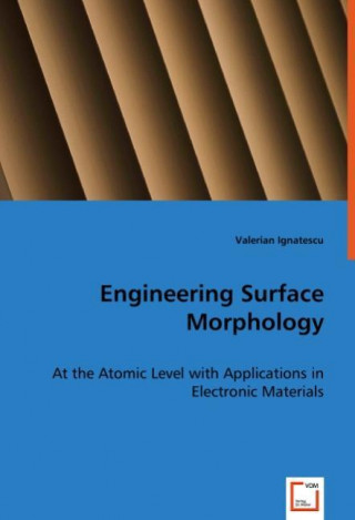
The silicon (111) and (001) surfaces have wide technological importance. Control of the morphologies of these surfaces at the atomic level is vital for such applications as layer-by-layer growth of epitaxial overlayers or assembly of nano-scale devices. By creating large areas with no or widely spaced atomic steps on patterned silicon surfaces by ultra-high vacuum (UHV) annealing, surface structures generated by surface premelting can be analyzed by simple quenching. The early roughness variation as a function of temperature and the morphologies that develop close to the boundaries of etched craters on Si(111) during UHV processing were also studied. Two applications using the substrates processed by UHV annealing were described. First, MOS capacitors were built on three types of Si(111) surfaces viz. atomically flat surfaces, stepped surfaces cleaned in UHV, and normal, RCA cleaned wafer surfaces. As expected, the smoother the Si substrate, the lower is the leakage current. In another application, Si(111) substrates with regular arrays of atomic steps were used to induce azimuthal alignment of crystals in thin polycrystalline pentacene films.


Sobre el libro
Inglés

Regale este libro hoy
Es fácil
1 Añadir al carrito y elegir Entregar como regalo en el checkout 2 Le enviaremos un vale 3 El libro llegará a la dirección del destinatarioTambién puede interesarle


 /
/
 Tapa blanda
 15.59
€
15.59
€
¡Hola! Soy Libroamiko, tu asesor de libros.
¿Cómo puedo ayudarte?